The compensator design webtool generates the compensation networks for the AD8450 and AD8451 controllers. The webtool assumes that the system uses a switching power converter.
To use the design webtool, follow these steps:
Enter the power converter and analog front-end parameters in the Plant Input Parameters section.
If the system uses an input filter before the PGIA and/or PGDA, or if the transfer function needs to be modified to incorporate non-modelled singularities, enter the extra transfer function in the Filter Transfer Function section.
Examine the design results in the Compensator (middle) section.
If needed, adjust the poles and zeros and component values of the compensator in the Compensator Poles and Zeros and the Compensator Component Values sections.
Examine the Bode plots of the Plant, Compensator and system's Loop Gain in third (right) section of the tool.
The System Infomation section provides performance metrics for the system loop gain.
For further help, click on the help icons of each section of the tool.
The webtool has an input validation algorythm that checks for invalid inputs. Valid inputs include engineering notation (T, G, M, Meg, MM, K, k, m, U, u, N, n, P, p, F, f, A, a), scietific notation (e.g 1.2e-3 or 1.4E3), or general notation.
Battery Charge/Discharge System Overview and Background Information
Figure 1. Battery Charge/Discharge System.
In battery formation and test system, each charge/discharge unit is comprised of three major components - an analog front end, a controller, and a power converter. These components form the CC and CV feedback loops that control the battery voltage and current during the charge/discharge process.
The analog front end measures the battery voltage and current, and feeds the measured values to the controller. The controller compares the measured battery voltage and current to the target values and generates the control signal for the power converter using the CC-CV algorithm. The power converter generates the battery current based on the applied control signal.
Figure 1 shows a simplified charge/discharge unit using an AD8450 or an AD8451 analog front end and controller. In this configuration, the power converter extracts power from a common DC voltage bus which can be shared by multiple charge/discharge units. The shunt Resistor (RS) converts the battery current (IBAT) into a voltage across it (VRS) that can be read by the AD8450 or the AD8451. The battery voltage is read directly from the battery terminals. In both measurements, Kelvin connections to the shunt resistor and the battery terminals reduce errors due to voltage drops in the wires. Voltage sources ISET and VSET set the target current and voltage for the CC and CV feedback loops, while the external compensation networks set the frequency response of the controller.
Figure 1 shows a simplified nonisolated synchronous buck/boost switching converter. The control signal (VCTRL), which is generated by the controller (AD8450 or AD8451), sets the duty cycle of the MOSFET switches and the average value of the voltage at node VM, by means of the converter’s PWM (ADP1972 or ADP1974). The inductor (LO) and capacitor (CO) form an LC low-pass filter that averages the voltage at node VM to generate a low ripple output voltage (VO) and output current (IBAT).
The non-isolated buck/boost converter is a bidirectional power converter that enables energy recycling in the system. During charge mode, the converter is run in buck mode, such that it pulls current from the DC bus to charge the battery. In discharge mode, the converter is run in boost mode, such that it pulls current from the battery and feeds it to the DC bus. Therefore, in boost mode, the energy stored in the battery is recaptured.
Switching Power Converter Linearized Model
Figure 2. Averaged Linearized Circuit for the Non-isolated Synchronous Buck/Boost Converter.
Figure 2 shows the averaged linearized circuit of the synchronous non-isolated buck/boost converter. In this model circuit, the DC voltage bus, the PWM and the switches are modeled as a linear amplifier with a voltage gain of AV. In buck mode (charge mode), the gain of the amplifier is VIN / VRAMP, where VIN is the voltage of the DC bus and VRAMP is the peak to peak voltage of the PWM ramp (4VPP in the ADP1972). In boost mode (discharge mode), the gain of the amplifier is -VIN / VRAMP. The linearized circuit in Figure 2 includes the parasitic resistance of the output inductor, RL, and the parasitic resistance of the output capacitor, RC f the power converter because they affect the transfer function of the converter. The shunt resistor RS and the ESR of the battery RB act as the load the power converter output.
The controller's PGIA gains the voltage across the shunt resistor by GIA and the controllers PGDA gains the battery voltage by GDA.
Switching Power Converter Bode Plot
Figure 1. Bode Plot of the Linearized Model of the Non-isolated synchronous Buck/Boost Converter.
The averaged linearized model of the buck/boost converter is a second order system with two poles and one zero. The two poles are generated by the LC filter, while the zero is caused by the series resistance of the output capacitor. Depending on the values of the circuit components, the transfer function of the model may be overdamped or underdamped. In the underdamped case, the poles are located at the resonant frequency of the LC filter, while, in the overdamped case, the poles may not be coincident. Figure 1 shows an approximate bode plot of the buck/boost converter with overdamped poles. The converter's LC filter poles are located at FPP1 and FPP2, and the zero is loacated at FPZ.
Filter Transfer Function
This section allows the modification of the plant's transfer function. The original plant's tranfer function is multiplied by the transfer function F(s), such that:
$${G}_{P-MOD}(s)=F(s)\cdot {G}_{P-ORIG}(s)$$
where, GP-MOD(s) is the modified plant transfer function, F(s) is the extra transfer function, and GP-ORIG(s) is the original plant transfer function generated by the parameters defined in the section Plant Input Paramenters.
The transfer function F(s) may represent the transfer function of the input filters that filter the voltage across the shunt resistor (VRS) and the voltage across the battery (VBAT). Also, F(s) may be used to modify the original plant transfer function in order to account for a more complex battery model.
Instructions
To use the filter transfer function feature, follow these steps:
Activate the Filter Transfer Function feature by selecting YES in the Extra TF in Loop field.
Enter the numerator of transfer function F(s) in the Numerator field and the denominator in the Denominator field. Input the numerator and denominator coefficients via comma separated lists with the highest order cofficient first and the lowest coefficient last. In other words, if the numerator is entered as 'a0 , a1 , ... , aN-1 , aN' and the denominator is entered as 'b0 , b1 , ... , bM-1 , bM', then:
$$F(s)=\frac{a_0s^N+a_1s^{N-1}+...+a_{N-1}s+a_N}{b_0s^M+b_1s^{M-1}+...+b_{M-1}s+b_M}$$
Disclaimer
The filter transfer function feature allows the webtool to show the effects of the added transfer function, but does not compensate its effects. Therefore, compensation of the new plant transfer function must be done manually by modifying the values in the compensation section.
Compensator Poles and Zeros
The webtool supports Type II and Type III compensators, and chooses between them automatically based on the input parameters. The tool uses the following decision rule:
If fPZ × 3 ≤ fC, implement a Type II compensator.
If fPZ × 3 ≥ fC, implement a Type III compensator.
Instructions
After choosing the compensator, the tool calculates the locations of the compensator poles and zeros automatically. These frequencies can be adjusted manually by changing the values of the corresponding fields.
Type II Compensator
The Type II compensator implements a pole at the origin, a zero at a frequency below the system’s cross-over frequency, and a high frequency pole. This compensator is used in cases where the magnitude of the uncompensated system is rolling off at -20 dB/dec at the desired cross-over frequency FC. Figure 1 shows the Bode plot of the uncompensated system or Plant, GP(s), the Type II compensator, GC(s), and the compensated system, L(s), respectively.
The zero of the Type II compensator is located at FCZ1 = FPP1 / 2, and the poles are located at FCP1 = FS / 2 and the orgin.
Figure 1. Bode Plot of the Plant, the Type II Compensator, and the Compensated System.
Type III Compensator
The Type III compensator implements a pole at the origin, two zeroes at frequencies below the system’s cross-over frequency, and two high frequency poles. This compensator is used in cases where the magnitude of the uncompensated system is rolling off at -40 dB/dec at the desired cross-over frequency FC. Figure 2 shows the Bode plot of the uncompensated system or Plant, GP(s), the Type III compensator, GC(s), and the compensated system, L(s), respectively.
The zeros of the Type III compensator are located at FCZ1 = FPP1 and FCZ2 = FPP2, and the poles are located at FCP1 = FPZ, FCP2 = FS and the orgin.
Figure 2. Bode Plot of the Plant, the Type III Compensator, and the Compensated System
The high frequency poles of the Type II and Type III compensators are usually placed at a frequency between FC and FS. These poles help attenuate the power converter’s output ripple without significantly affecting phase margin of the compensated system.
Compensator Component Values
The webtool supports inverting and noninverting op-amp circuit implementations for the Type II and Type III compensators. After choosing the required compensator type and calculating the location of the compensator poles and zeros, the tool calculates the component values for the op-amp circuit implementation. For extra flexibility, these values can be adjusted manually by changing the values of the corresponding fields. The equations used by the webtool to calaculate the component values can be found at AN-1319: Compensator Design for a Battery Charge/Discharge Unit Using the AD8450 or the AD8451.
For further help on the op-amp circuit implementations, click on the help icon in the op-amp circuit figure on the main display or click here.
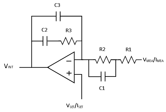
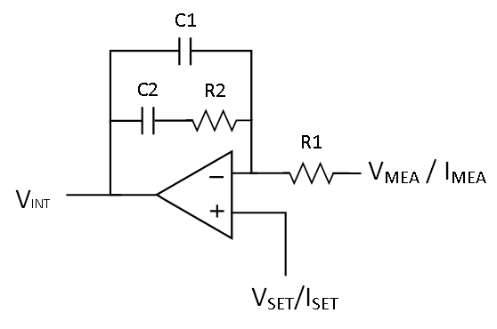
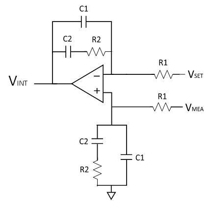
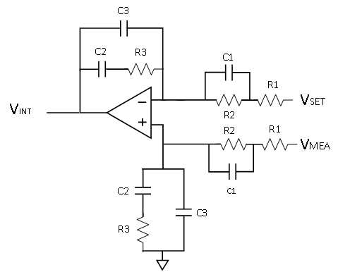
Compensator Implementation
The op-amp circuit implementation of the compensator is formed by the loop filter amplifiers included in the AD8450 and AD8451, and the user provided external compensator network. The loop-filter amplifiers can be configured to implement inverting and noniverting Type I, II and III compensators as shown in the figures below. Note that the webtool only supports Type II and III compensators.
Compensator Circuits and Transfer Functions
The table below shows the supported op-amp circuit compensator implementations with their respective transfer functions:
The webtool shows the compensator design results in three plots and one optional plot:
Plant: Bode plot of the plant transfer function including the modifications from the filter transfer function, F(s).
Compensator: Bode plot of the compensator transfer function.
Filter: Bode plot of the Filter transfer function, F(s), (only if the filter feature is active).
Loop Gain: Bode plot of the system's loop gain, L(s).
To view one of the result Bode plots, simply click on the appropriate tab.
The vertical red line in the plots is the cross-over frequency of the system. The blue lines show the phase loss of the plant, the phase gain of the compensator and the phase margin of the system.
Loop Gain Information
This panel shows the stability metrics of the system's Loop gain, L(s). These metrics include:
Cross-over Frequency: The bandwidth of the system. This is set to one tenth of the switching frequency, FS / 10.
Phase Margin: Phase Margin of the system. The tool's algorythm guarantees a phase margin of at least 60°.
Gain Margin: Gain Margin of the system and the -180° phase frequency.
To do list
Add HELP window contents - DONE
Add title atributes where needed
H-Mirror the images
Add links to Datasheets - DONE
Add links to AN-1319 - DONE.
Fix Google Analytics
Questions for Anne
Feedback on Error handling.
Compensation Script
Parse Engineering notation. - DONE
Validation
Do further testing: C0=1k, L0=1k - DONE
Final Clean Up
Remove Old Instruction Div - DONE
Remove Old Instruction function toogle in script.js - DONE
 Plant Input Parameters